< MEMORY >

In computer systems, memory generally refers to Random Access Memory (RAM), which is used to temporarily store data that is actively being used or processed by the system. RAM is capable of storing and retrieving n-bits of data, where "n" indicates the bit width of the system's memory operations (e.g., 8-bit, 16-bit, 32-bit, etc.). When data is input into the system, it is assigned a unique memory address. Each memory location in RAM can hold a specific number of bits of data, and the R/W (Read/Write) control signal determines whether data is being read from or written to a particular memory address. This ability to access any location directly (hence "random access") is what distinguishes RAM from other types of memory like sequential storage devices (e.g., hard drives or tapes), which require data to be accessed in a fixed order.

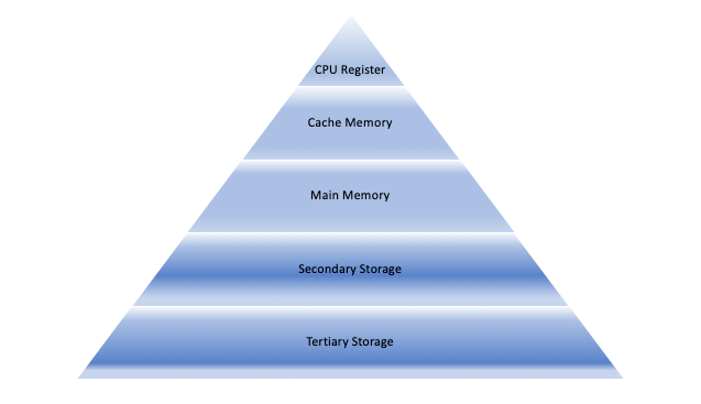
< Memory Hierarchy >

Memory hierarchy is a concept in computer architecture that organizes memory storage based on various characteristics such as access speed, size, and cost. The idea is to provide fast access to the most frequently used data while managing larger, slower storage devices for less frequently used information. Memory hierarchy structures typically have multiple levels, each offering different trade-offs in terms of response time, capacity, and cost. These levels are organized from the fastest, smallest, and most expensive memory at the top, to the slowest, largest, and cheapest memory at the bottom.
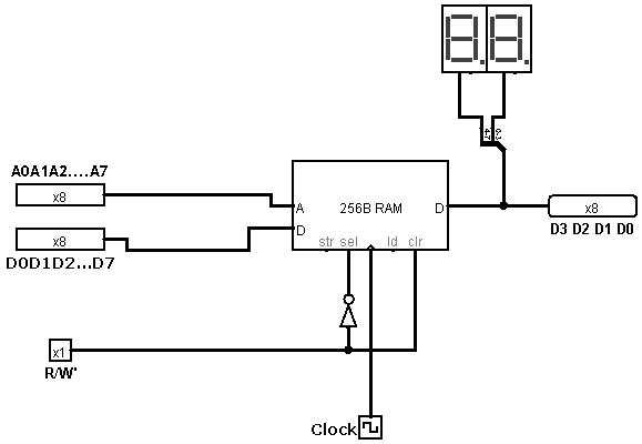
<Diagram >

Main Image

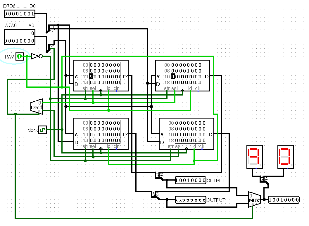
< MEMORY OF SIZE 256×8 USING 256x4 >

Main Image

< Challenges Faced >

  • Grasping the concept of memory hierarchy (registers, cache, main memory, secondary storage) and how data moves between these levels.
  • It requires understanding trade-offs between speed, size, and cost across different memory types.
  • Learning about cache organization (direct-mapped, fully associative, and set-associative) and replacement policies (LRU, FIFO, etc.) Balancing performance with complexity, and understanding how caches improve speed but introduce design overhead..
  • Determining the correct number of address lines for the required memory size.
  • Managing read and write operations with control signals (enable, read, write).
  • Synchronizing memory operations with clock signals.

< Learning Outcomes >

  • Gained insight into memory organization, including RAM, ROM, and the role of address lines in determining memory size.
  • Learned how to configure memory addressing using decoders and address lines to map data correctly to memory locations.
  • Understood how to synchronize read and write operations using control signals and clock pulses.
  • Improved my ability to troubleshoot and debug complex memory circuits, identifying and fixing common errors like data corruption and misaddressing.
  • Learned how memory systems integrate with processors and other components, emphasizing compatibility in data width and control logic.