<Design an 8-bit processor using 2-address format for immediate addressing mode

ALU: An 8-bit Arithmetic Logic Unit


An 8-bit ALU is like a mini math genius inside a computer chip that works with 8-bit numbers. These numbers are sequences of 8 zeros and ones, meaning it can handle values ranging from 0 to 255. The ALU is really skilled at math and logical operations, such as:
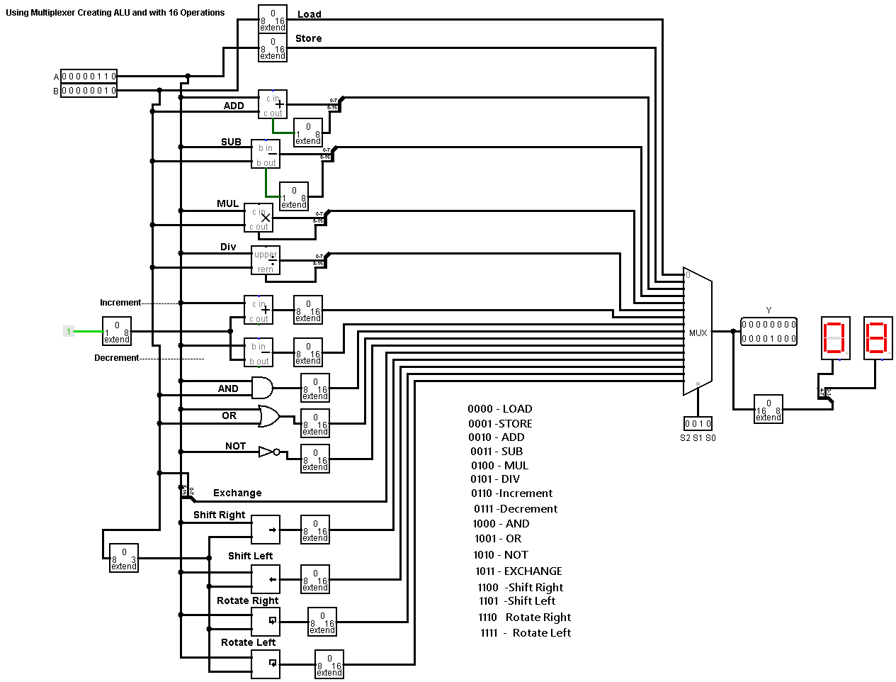
  • Addition and Subtraction: Solving math problems like a calculator.
  • Logical Operations: Performing tasks like AND, OR, and XOR, which help the computer make decisions.
  • Shifting: Moving bits left or right, which is useful for tasks like multiplying or dividing by powers of 2.

<Diagram >

Main Image

< Program Counter (PC) >

The Program Counter (PC) is a vital register in a computer's processor, overseeing the memory address of the upcoming instruction and guiding the sequential execution of a program.
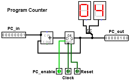
  • Instruction Address Management: Tracks the memory address of the next instruction to be executed and guides the processor through a program sequentially.
  • Control Flow Handling: Manages branches and jumps, enabling the execution of non-linear code. Handles function calls and returns, ensuring the program returns to the correct address.
  • Interrupts and Exceptions: Dynamically adjusts to external events, such as hardware interrupts or errors, to respond appropriately.
  • Fetch-Decode-Execute Cycle: Plays a pivotal role in orchestrating the systematic execution of program instructions and ensures the processor fetches the correct instruction in the sequence.
  • Clock Synchronization: Swiftly updates output values with each clock cycle, keeping the processor aligned with system timing for smooth operation.
  • Reset Functionality: Clears its contents when a reset signal is triggered, providing a clean slate for restarting or beginning a new operation.
  • Program Integrity: As a central component, it ensures that instructions are executed in the correct order, maintaining program reliability.
Main Image

< Register Bank >

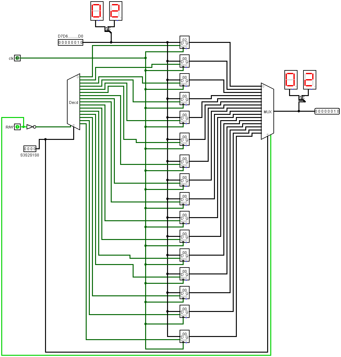
The register file in an 8-bit processor is a collection of 16 general-purpose registers, each capable of storing 8-bit data. These registers serve as small, high-speed storage units that the CPU can quickly access during processing tasks, enabling efficient execution of instructions and temporary data storage.
The register file in an 8-bit processor consists of 16 general-purpose registers (R0 to R15), each capable of storing 8-bit data. These registers are selected using a 4-bit binary address :

Storing Data in Registers

When a specific register is selected (e.g., R0 with address 0000), the processor can write 8-bit data into that register. The write operation is triggered by a control signal, allowing the data to be stored in the selected register.
Main Image

< Control Unit>

The Control Unit (CU) is a fundamental part of a computer's processor that acts as the central command center for coordinating all operations. Its primary function is to direct the flow of data and instructions within the processor, ensuring that tasks are executed in the correct sequence and at the right time.
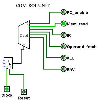
  • Program Counter (PC) Enable:: Activates the Program Counter to provide the address of the next instruction to fetch.
  • Memory Read: Sends a signal to retrieve data or instructions from memory into the processor.
  • Instruction Register (IR) Load: Transfers the fetched instruction into the Instruction Register for decoding.
Main Image

< Processor Design >

Main Image

< Working >

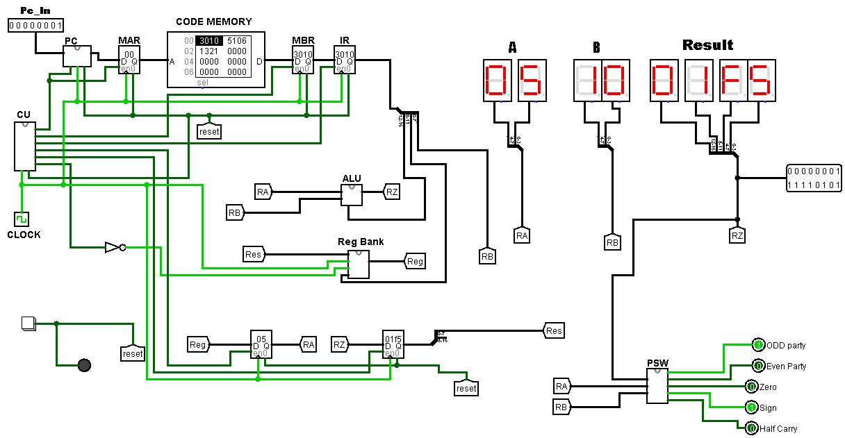
This diagram represents the architecture of an 8-bit processor using a 2-address format for immediate addressing mode, where instructions involve operations between a constant value (immediate data) and a register. Here's an explanation of how this processor operates:

Program Counter (PC): Holds the address of the next instruction to execute. It increments automatically unless a jump or branch modifies it.

Memory Address Register (MAR): Receives the address from the PC and sends it to memory to fetch instructions or data.

Memory Buffer Register (MBR): Temporarily holds fetched data or instructions from memory.

Instruction Register (IR): Stores the current instruction for decoding and execution.

Control Unit (CU): Decodes the instruction and generates control signals for execution. It orchestrates operations like PC enable, memory read, instruction fetch, and operand fetch.

Register Bank: Contains general-purpose registers (e.g., RA, RB) to store operands and results. RZ is used for storing ALU results.

Arithmetic Logic Unit (ALU): Performs arithmetic (e.g., addition, subtraction) and logical operations (e.g., AND, OR, XOR). It takes inputs from the register bank and stores results in RZ.

Clock: Synchronizes all operations and ensures sequential execution of instructions.

Example Execution: If the instruction is ADD RA, #05, the processor will:
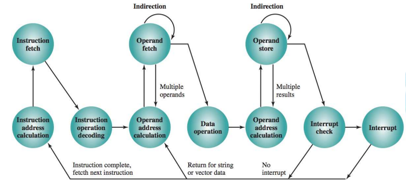
  • Fetch the instruction using the PC and store it in the IR.
  • Decode the instruction and identify operands (RA and #05).
  • Fetch the immediate value and perform the addition in the ALU.
  • Store the result back in RA.

< Instruction Life Cycle >

< Microinstructions >

Instruction: LOAD R0, #05
Microinstructions:

  • T1: MAR ← (PC); CU issues Read command
  • T2: MBR ← (memory); PC ← (PC) + 1
  • T3: IR ← (MBR)
  • T4: ACC ← #05
  • T5: R0 ← (ACC)

Instruction: ADD R2, #03
Microinstructions:

  • T1: MAR ← (PC); CU issues Read command
  • T2: MBR ← (memory); PC ← (PC) + 1
  • T3: IR ← (MBR)
  • T4: ACC ← (R2) + #03
  • T5: R2 ← (ACC)

Instruction: SUB R3, #02
Microinstructions:

  • T1: MAR ← (PC); CU issues Read command
  • T2: MBR ← (memory); PC ← (PC) + 1
  • T3: IR ← (MBR)
  • T4: ACC ← (R3) - #02
  • T5: R3 ← (ACC)

< Challenges Faced >

  • Instruction Encoding: Designing an efficient instruction set and encoding scheme for the 2-address format with immediate addressing mode requires careful planning to balance opcode size, address fields, and immediate values.
  • Operand Fetching: Managing the fetching of operands, especially immediate values, involves creating a circuit that can efficiently fetch and process these values from memory or directly from the instruction.
  • ALU Operations: implementing Arithmetic Logic Unit (ALU) operations with immediate values involves circuits capable of performing arithmetic operations on both registers and immediate values. This demands careful design to ensure compatibility and precision.
  • Register File Design: The design of the register file needs to accommodate the storage and retrieval of 8-bit data for two operands, considering the 2-address format.
  • Data Path Complexity: integrating the data path for immediate addressing increases complexity, requiring a well-organized circuit to handle both register-to-register and immediate value operations seamlessly.
  • Instruction Execution Timing: Coordinating the timing of instruction execution becomes crucial to maintain proper synchronization between various stages of the processor pipeline, especially when dealing with immediate values.
  • Control Unit Challenges: The control unit must be designed to generate appropriate control signals for the ALU, register file, and other components based on the specific needs of the 2-address format with immediate addressing mode.

< Learning Outcomes >

  • Trade-off Between Operand Fields and Instruction Length: I learned how to balance the size of the opcode, operand fields, and immediate values to ensure that the instruction format remains efficient, given the 8-bit constraint. This includes the challenge of fitting operands and operations within a limited bit space.
  • Handling Immediate Addressing Mode: I gained an understanding of how immediate addressing mode simplifies memory access by directly embedding operands into the instruction. This helps in reducing memory fetch cycles and makes instructions faster.
  • ALU Flexibility: I learned the importance of designing an ALU that can process both register-based and immediate operands. This required understanding how to integrate different data sources into the ALU without increasing its complexity too much.
  • Control Unit Complexity: The process of designing the control unit helped me understand how complex it can be to manage different types of instructions (those involving registers and immediate values) and generate control signals to execute those operations properly.